Scanning Tunneling Microscopy (STM) is a type of microscope used for imaging surfaces at the atomic level.
It is based on the principle of quantum tunneling and was invented by Heinrich Rohrer and Gerd Binnig in 1981,
for which they were awarded the Nobel Prize in Physics in 1986.
STM has had a major impact across physics, chemistry, and materials science, transforming our understanding of surface structures, electronic properties, and nanoscale phenomena.
As a non-optical technique, it enables precise investigation and manipulation of matter, opening new possibilities in nanomaterials and nanodevice research.
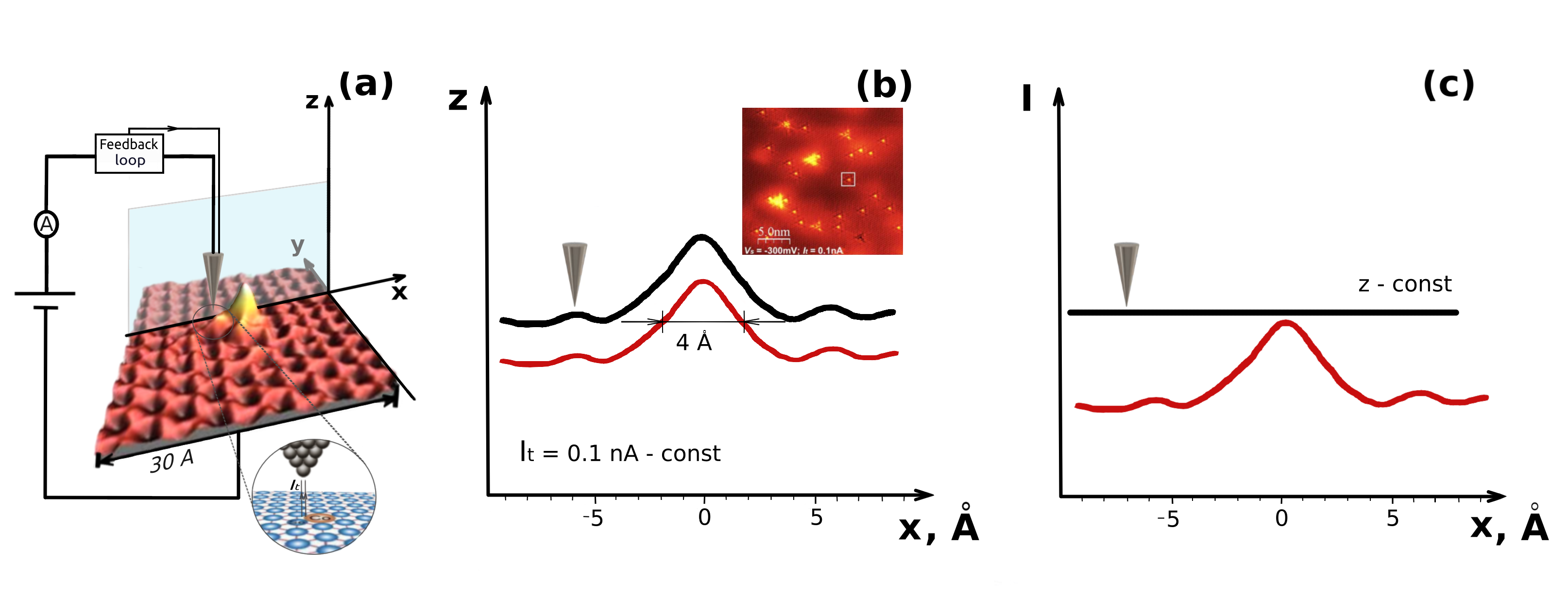
The figure below shows a schematic of a typical STM system (adapted from [M. Ye et al.]). A sharp metallic tip is positioned just a few angstroms above the sample surface, and its position in three dimensions is precisely controlled by piezoelectric elements. When a bias voltage is applied, a tunneling current arises due to the quantum tunneling of electrons between the tip and the sample. This current is extremely sensitive to the tip–sample distance and reflects both the surface topography and electronic structure.
STM Operational Modes:
- Imaging mode: This mode includes two scanning regimes used to achieve atomic-resolution imaging of the sample surface morphology:
- Constant-current mode (Fig.(b)): A feedback loop maintains a constant tunneling current between the tip and sample at each lateral position \((x,y)\). As a result, the tip's \(z\)-position is continuously adjusted during scanning.
- Constant-height mode (Fig.(c)): The tunneling current is measured at a fixed vertical position \(z\) of the tip.
-
Spectroscopy mode: In this mode, the tunelling current \(I\) is monitored as a function of varying parameters \(z\) or \(V\):
- \(I(z)\) spectroscopy: The tip-sample distance \(z\) is varied at a fixed voltage \(V\). This method is useful for characterizing the quality, sharpness, and cleanliness of the STM tip.
- \(I(V)\) spectroscopy: The tunneling current is recorded as a function of the applied voltage \(V\), which provides insights into the electronic structure of the surface, including barrier heights, local density of states, and molecular motion modes.
- Manipulation mode: This mode enables deliberate manipulation of atoms and molecules on the sample surface using the STM tip. By applying voltage pulses or carefully adjusting the tip-sample distance, individual atoms or molecules can be picked up, moved, and positioned with high precision. This allows for the construction of nanostructures, investigation of surface reactions, and real-time study of atomic-scale processes.

\(z \leq 0\) and \(U(z) = 0\):
\(\psi_s(z) = e^{ikz} + Ae^{-ikz} \) - incoming wave + reflected wave;
\(0 < z < d\) and \(U(z) = U\)
\(\psi_b(z) = Be^{-\varkappa z} + Ce^{\varkappa z}\) - decaying in barrier;
\(z < d\) and \(U(z) = 0\):
\(\psi_t(z) = De^{ikz} \) - transmitted wave;
where \(k = \frac{\sqrt{2mE_0}}{\hbar}\) and \(\varkappa = \frac{\sqrt{2m(U - E_0)}}{\hbar}\) - the decay constant.
The coefficients A, B, C and D result from the wave function continuity condition at two interface.
The following variables were used for calculations:
\(U = \) eV
\(E = \) eV
\(d_p= \) Å
\(A\)
\(B\)
\(C\)
\(D\)
The transmission coefficient \(T\) represents the probability flux of a particle passing through a potential barrier:
$$T = \frac{|\psi_{t}(z)|^2}{|\psi_{s}(z)|^2} $$
- In Tunneling regime, where the particle energy \(E < U\): $$T = DD^* = \left(\cosh ^2(\varkappa d)+\frac{1}{4} \left(\frac{\varkappa}{k} - \frac{k}{\varkappa}\right)^2 \sinh^2 (\varkappa d)\right)^{-1}.$$
- Near the Barrier Top (\(E = U\)) , when \(\varkappa \rightarrow 0\), the barrier becomes effectively transparent, and the transmission coefficient \(T\) is given by: $$T = \frac{4(1 + k^2d^2)}{4 + k^2d^2}. $$
- In the Over-barrier regime (\(E > U\)), the particle propagates over the barrier, and both the wavefunction and transmission coefficient become oscillatory: $$T = \left[1 + \frac{1}{4} \left(\frac{k'}{k} - \frac{k}{k'}\right)^2 \sin^2(k'd)\right]^{-1},$$ where \(k' = \frac{\sqrt{2m(E - U)}}{\hbar}\).
In the limit where \(E << U\) and the barrier is wide (\(\varkappa d >> 1\)), the expression for the transmission coefficient simplifies to: $$T = T_0 \exp{\left(-\frac{2d}{\hbar}\sqrt{2m(U - E_0)}\right)},$$ where \(T_0 = 4\left[1 + \frac{1}{4} \left(\frac{\varkappa}{k} - \frac{k}{\varkappa}\right)^2\right]^{-1}\).
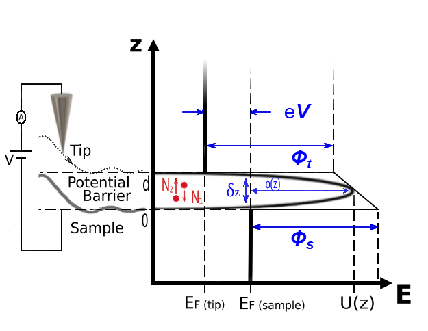
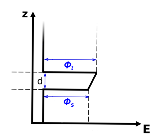
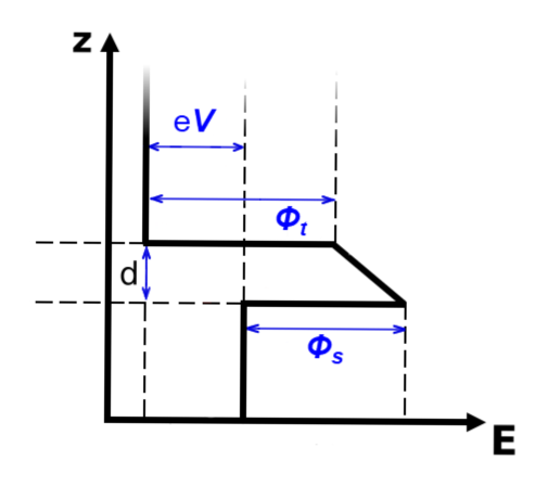
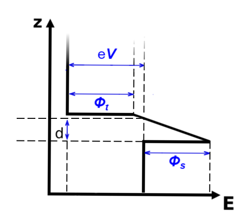
To simulate the spectroscopy regime (i.e., the (\(I(V))\) characteristic) of a Scanning Tunneling Microscope, we consider a Metal-Insulator-Metal system with an arbitrarily shaped potential barrier. The applied bias voltage \(V\) induces a tunneling current that depends on the energy density of states \(n(p_z)\) and the transmission probability \(T(E_z)\) for electrons traversing a barrier of height \(U(z)\). The quantities \(N_1\) and \(N_2\) represent the number of electrons tunneling through the barrier in opposite directions, determining the net current. \(\Phi_t\), \(\Phi_s\) are the work functions of the tip and sample materials, respectively.
Following the approach described in [John G. Simmons], the dependence \(I(V)\) is obtained using the WKB approximation, which allows us to derive an expression for the tunneling current density:
where \( J_0 = \frac{e}{4\pi^2\beta^2\hbar} \) and \( A = 2\beta\sqrt{\frac{2m}{\hbar^2}}\), \(e\) is the elementary charge, \(δ_z\) is the width of the potential barrier for electrons at the Fermi level, \(\bar \phi\) is the average barrier height, defined as: \(\bar \phi = \frac{1}{\delta_z}\int_{z_1}^{z_2}{\phi(z)\,dz}\), and \(\beta\) is a correction factor dependent on the bias voltage.
To generate the \(I(V)\)characteristics, it is necessary to determine the relevant barrier parameters and select an appropriate maximum applied voltage.
The following variables are used for calculations :
\(\Phi_s = \) eV;
\(\Phi_t = \) eV;
\(d = \) Å ;
\(S = \) nm\(^2\);
\(V_{max} = \) V;
The corresponding energy diagram of the Metal-Insulator-Metal (MIM) system is displayed on the left.
The rapid advancement of materials science, nanotechnology, and biotechnology requires ongoing development in high-resolution instrumentation, fabrication methods, and analytical tools for manipulating and characterizing matter at atomic and molecular scales. The Scanning Tunneling Microscope (STM) is one such tool that addresses these needs.
Several key applications of STM are demonstrated below:
- Application of STM in Electrocatalysis and Electrochemistry: STM enables atomic-level characterization of electrocatalyst surfaces and the study of electrochemical interfaces with reactants, even under ultra-high vacuum or harsh conditions. This capability is demonstrated in the work by H. Feng et al.
-
STM plays a crucial role in the development of technologies across various scientific fields, such as nanoparticle synthesis, biological deposition, ultra-thin film growth, and surface engineering. These processes rely on precise surface preparation, morphology control, and atomic-scale characterization. For example, in the study by Yu Wang et al., STM was used to investigate the Cu(111) surface for catalysis and two-dimensional material growth. This study systematically analyzed morphological and structural changes after ion bombardment and annealing between 300-740°C using in situ low-temperature STM.
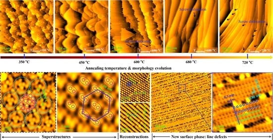 The morphology and structure changes of the Cu(111) surface after treatment by ion bombardment and annealing with a temperature range of 300-720 °C [Z.Qu et al. Nanomaterials 12, P.4278 (2022). Licensed under CC BY 4.0.]
 - The first quantum calculations using individual titanium atoms on a surface were successfully performed by controlling them with microwave signals emitted from an STM, as demonstrated by Yu Wang et al. in their study. This technology holds significant potential for developing a new type of quantum computer. By precisely manipulating atomic spins, the researchers implemented a simple two-qubit quantum operation and successfully read out the results.
-
The article by J. Seibel et al. discusses the use of scanning probe microscopy, including STM, to characterize biomolecules such as DNA and individual biopolymers by resolving the surface morphology and electronic properties of DNA strands deposited on conductive substrates.
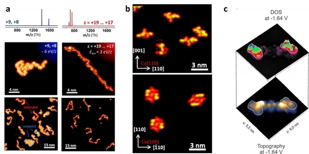 STM imaging of peptides [J. Seibel et al. ChemPhysChem 25, P.e202400419 (2024). Licensed under CC BY 4.0.]
| Technique | Resolution | Imaging Principle | Sample Requirement | Information Provided |
|---|---|---|---|---|
| STM (Scanning Tunneling Microscope) | Atomic-scale (~0.1 nm) | Quantum tunneling current measurement | Conductive or semiconductive surfaces | Topography, electronic structure |
| AFM (Atomic Force Microscopy) | Atomic-scale (~0.1 nm) | Measures forces between tip and sample surface | Conductive or insulating | Topography, force interactions |
| SEM (Scanning Electron Microscopy) | ~1–10 nm | Electron beam scans surface, detects secondary electrons | Conductive or coated samples | Surface morphology |
| TEM (Transmission Electron Microscopy) | Sub-atomic (< 0.1 nm) | Electron beam transmitted through thin sample | Ultra-thin samples | Internal structure |